GaN Single Crystal

GaN -Single Crystal Substrate,N-type, (0001), 10x10.5x0.3 mm , 1SP

GaN -Single Crystal Substrate,N-type, (0001), 10x10.5x0.3 mm , 1SP

기본 정보
Product Name GaN -Single Crystal Substrate,N-type, (0001), 10x10.5x0.3 mm , 1SP
Sale Price Call for Price
Product Code GaNC101003S1US
Quantity 수량증가수량감소
상품 옵션
 

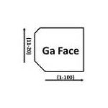
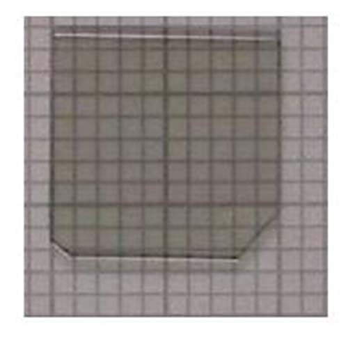
GaN single crystal substrates is made by a hydride vapor phase epitaxy (HVPE)-based method. During the HVPE process, HCl reacts with molten Ga to form GaCl, which in turn reacts with NH3 to form GaN. The large growth rate enables the growth of self-supporting wafer thicknesses in a convenient time period.

Specifications of the Substrate

  •      •  Orientation:                          c-axis (0001) +/- 1.0 o
  •      •  Type:                                    N-type(undoped)
  •      •  Nominal Thickness              300+/- 25 microns
  •      •  Dimension:                          10 mm x 10.5 mm +/- 0.5 mm
  •      •  Resistivity                            <0.5 ohm.cm
  •      •  Dislocation Density              < 5x10^5 cm^-2
  •      •  TTV:                                     <=15 um
  •      •  BOW:                                   <=20 um
  •      •  Front Surface Finish           (Ga Face) , RMS <2.0 nm, Epi-Ready polished 
  •      •  Back Sutface Finish:           Fine Ground                                         
  •      •  Useable Surface area:        >90%
  •      •  Package Single Wafer Container or membrane box 
  •      •  For XRD & AFM data, please click here