| |
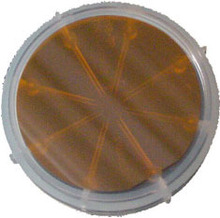
GaP Substrates (111)
GaP Wafer, undoped (111)B 2"x0.4 mm, 2sp,Semi-Insulating
Specifications:
- • GaP single crystal wafer,Semi-Insulating
- • Doping: undoped, Semi-insulating
- • Type of conductivity: N
- • Orientation: (111)B
- • Size: 2" diameter x 0.4mm
- • Polished: two sides polished, with P terminated side facing down in the box
- • Resistivity: 1 x 10^7 ohm.cm
- • Mobility: 160 cm^2/Vs
- • Carrier concentration: 3.9 x 10^9 cm^-3
- • EPD: 3.8 x 10^4 cm^-2
- • Surface finish (RMS or Ra) : < 8A
|
|
|

Working days : Monday to Saturday

|
|
|