| |
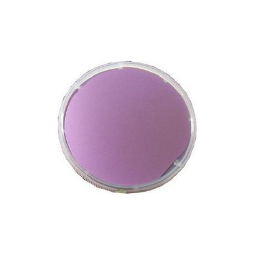
Thermal Oxide Wafer 4" Dia.
Thermal Oxide Wafer: 500 nm SiO2 Layer on Si (100), 4"dia x 0.50 mm t, N-type ,P doped 1sp ,0.01-0.1 ohm.cm (부가세 별도)
- •Research Grade , about 80 % useful area
•SiO2 layer on 4" Silicon wafer
•Oxide layer thickness: 500 nm ( 5000A) +/-10%
•Refractive index - 1.455
- Silicon Wafer Specifications
- Conductive type
- N-ype/ P-dped
- Size
- 4"meter +/- 0.5 mm x 0.5 mm
- Surface roughness, R
- < 5A (RMS)
- Optional
- you may need tool below to handle the wafer ( click picture to order )
|