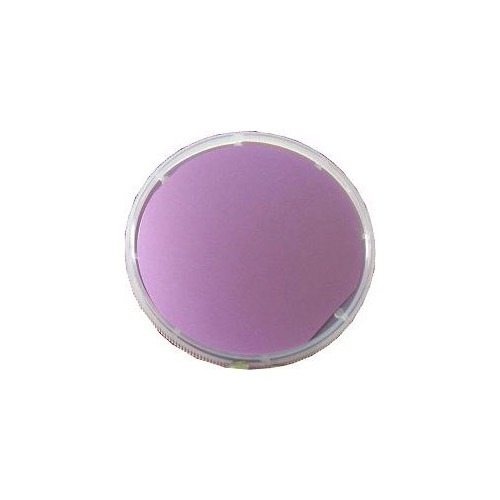
•Research Grade , about 80 % useful area •SiO2 layer on the FRONT SIDE (only) of 3" Silicon wafer •Oxide layer thickness: 100 nm ( 1000A) +/-10% •Growth method - Dry oxidizing at 1000oC •Refractive index - 1.455 •Note: customized oxide layer available upon request from 50 nm - 1000 nm
Silicon Wafer Specifications
Conductive type
P-ype/ B-dped
Resistivity
0.1-1.0 ohm.cm
Size
3" +/- 0.5 mm in diameter x 0.5 mm +/- 0.05 mm th
Orientation
(111) +/- 1o
Polish
one side polished
Surface roughness
< 5A
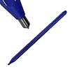
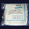
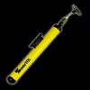
Optional
you may need tool below to handle the wafer ( click picture to order )