| |
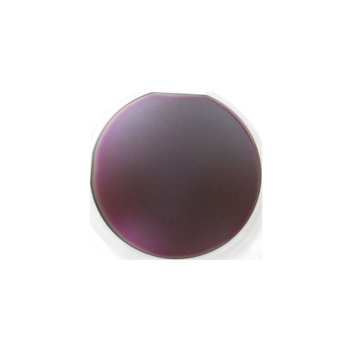
SiC Film(3C) on Si wafer
4" SiC-3C N type Film and CMP on both sides of Silicon (100) N-type Wafer after epitaxy growth, 3.2 micron film Thickness after polishing
Specifications:
- • Film: SiC film with 3C structure grown by PECVD
- º Thickness: 3200 nm +/- 10%
- º SiC (100)
- º Surface: CMP ( film chemical mechanical polished )
- º Target doping level: 1.0E17 - 1.0E18 /cc
- º Type and dopant: N type, Nitrogen doping
- º Surface defects density (microscopic inspection of crystallites or other macro-defects) <= 3E3cm^2
- º : 16
- • Silicon substrate:
- º Size: 100 mm dia x 0.525 mm thickness
- º Orientation: (100)
- º Type: N type / P doped
- º : 1- 10 ohm.cm (resistivities is dependent on the doping level)
- º Polish: Both sides optical polished
|
|
|

Working days : Monday to Saturday

|
|
|