InGaAs EPI on InP( Semi-insulating)

2" dia. InGaAs EPI Film on InP (SI) (100) Depositied by MOCVD (eg InP:Fe) 2" dia x0.35mm,2sp,Film:500 nm

2" dia. InGaAs EPI Film on InP (SI) (100) Depositied by MOCVD (eg InP:Fe) 2" dia x0.35mm,2sp,Film:500 nm

기본 정보
Product Name 2" dia. InGaAs EPI Film on InP (SI) (100) Depositied by MOCVD (eg InP:Fe) 2" dia x0.35mm,2sp,Film:500 nm
Sale Price Call for Price
Product Code InGaAs on InP(SEMI) 50D035C2-500nm--US
Quantity 수량증가수량감소
상품 옵션
 
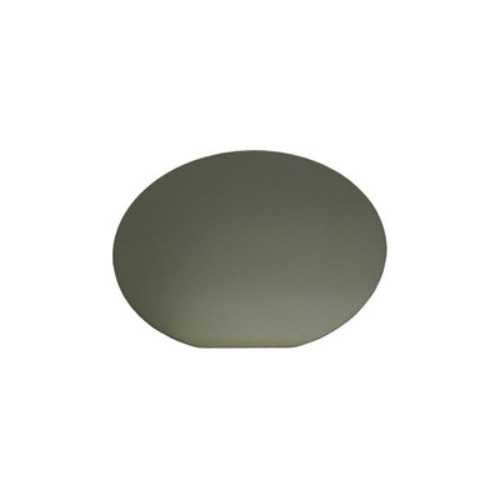
  • 2" dia. wafer InGaAs EPI on InP (Semi-insulating)(100) by MOCVD deposition
  •  Substrate
  • InP Orientation
  • (100)
  • Doped with Fe, Semi-Insulating
  • wafer Size
  • 2" diameter
  • Resistivity
  • > 1 x 10⁷ ohm.cm
  • EPD
  • < 1 x 10⁴ /cm2
  •  EPI Film
  • Lattice matched In/Ga alloy layer of N-type InGaAs(Si-doped),
    Nc > 2 x 10¹⁸ /cc
    Film Thickness :0.5 um (+/- 20%)
    Both Sides polished
    Roughness of epi-layer is close to 1 mono-layer (ML)
    One the back side we can expect some deposits and we can't guarantee the same quality (roughness) as in the case of active layer surface.
  •  EPI ready surface and packing
  •  Typical Properties
Dopant Type Carrier
Concentration
( cm-3 )
Mobility
( cm2/V.Sec )
Resistivity
( ohm-cm )
EPD
( cm-2 )
Undoped N 7.5 - 9.5 x 10¹⁵ 4300 - 4400 1.6E-1 - 4.5E-1 < 5000
Sn N 0.5 ~ 1.0 x 10¹⁸
0.5 ~ 1.0 x 10¹⁸
200 ~ 2400
1500 ~ 2000
0.001 ~ 0.002
0.0025 ~ 0.007
3 ~ 5 x 10⁴
Zn P 0.8 ~ 2.0 x 10¹⁸
2.5 ~ 4.0 x 10¹⁸
2500 ~ 3500
1300 ~ 1600
0.0025 ~ 0.006 1 ~ 3 x 10⁴
Fe Semi-
Insulating
N/A 1550 - 1640 (2.1 - 2.7) x 107 < 5000