| |
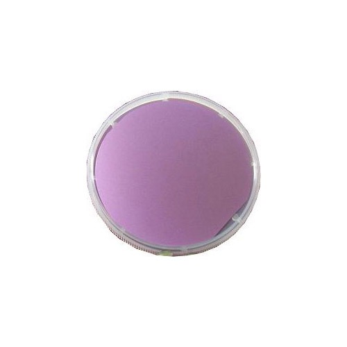
Thermal Oxide Wafer 2" Dia.
Thermal Oxide Wafer: 300 nm SiO2 Layer on Si (100), 2" dia x 0.50 mm t, P type B doped, 1 side polished, R:<0.005 ohm.cm
-
Research Grade , about 80 % useful area
- SiO2 layer on 2" Silicon wafer
- Oxide layer thickness
- 300 nm ( 3000 A ) +/-10%
- Growth method
- Dry oxidizing at 1000 oC
- Note
- customized oxide layer available upon request from 50 nm - 1000 nm
- Silicon Wafer Specifications
- Conductive type
- P type / Boron doped
- Size
- 50.8 diameter +/- 0.5 mm x 0.50 +/- 0.025 mm
- Surface roughness, Ra
- < 5A (RMS)
|