MTI KOREA Battery
Battery R & D
- Coin Cell Preparation
- Cylindrical and Prismatic Cell Preparation
- Pouch Cell Preparation
- Battery Test Equipment
- Consumables for Battery R&D Synthesis
- Thermoelectric Materials
- Zinc-Ion Batteries
Crystal & Material
Crystals Substrates : A-Z
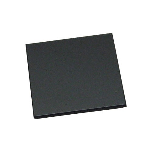
Ceramic Substrates : A-Z
Thin Film on Substrates : A-Z
Metallic substrate :A to Z
Nano Powder&Chemical
Target / Evaporation : A-Z
Thermal Processing
Smart Furnaces
- Muffle Furnaces (400-1800°C)
- Tube Furnaces (1- 7 Zones)
- CVD Furnace System
- Hi-Pressure & H2 Gas Furnaces & Hot Pressing
- RTP Furnaces
- Crystal Growth System
- Dry Ovens / Hot Plates
- Melting and Casting
Furnace Accessories
Plasma System
Plasma Sputtering & Cleaning
PECVD
Microspheres-Nanospheres
Inorganic
Organic
Magnetic
Radioactive
Size Standards
Sample Preparation & Analysis
Cutting / Dicing Saws
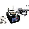
Polishing Machines
Lab Press & Rollers
Power & Slurry Mill / Mixer
Film Coating
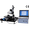
Desktop Machine-shop
Material Analysis
TGA Analysis
Battery / Capacitor Analyzers
Desk-Top X-Ray Instruments
Digital Microscopes
Other Lab Equipment
Glove Box & Fume Hood
Digital Lab Balances
Plasma/UV-Zone Cleaners
Ultrasonics/Water Circulator
UV Equipment & Adhesives
Lab Ware / Accessory
Sample Handling
Gel Sticky Boxes
Membrane Film Boxes
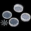
Round Wafer Carriers
IC Tray & Plastic Boxes
Vacuum Pen & Tweezers
Knowledge Center
Silicon Wafer Specifications