| |
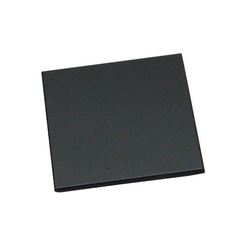
SiC Epi Film (3C) on Silicon Wafer
SiC-3C Undoped Epi Film as CMP on both sides of Silicon (100) Wafer after epitaxy growth, 2.2 micron Thick, 10x10x0.525 mm
Specifications
- • Film: SiC Epi film with 3C structure grown by PECVD
- º Thickness:2200 nm +/- 10%
- º Orientation: 3C SiC (100)
- º Surface: CMP ( film chemical mechanical polished ) on both sides with Ra < 5 Angstrom
- º Type and dopant: N type, Undoped
- º Surface defects density (microscopic inspection of crystallites or other macro-defects) <= 3E3cm^2
- º TTV: 5-29
- º Bow: -9 ~ 3
- • Silicon substrate
- º Size: 10x10 x 0.525 mm thickness
- º Orientation: (100)
- º Type:P type / B doped
- º Resistivity:1- 10 ohm.cm
- º Polish: Both sides optical polished
|