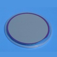
New substrate

SiO2+TiO2+Pt (111) Film on Si ,4"x0.525mm, 1sp P-type B-doped, (SiO2=300nm,TiO2=20nm ,Pt(111)=150nm)

SiO2+TiO2+Pt (111) Film on Si ,4"x0.525mm, 1sp P-type B-doped, (SiO2=300nm,TiO2=20nm ,Pt(111)=150nm)

기본 정보
Product Name SiO2+TiO2+Pt (111) Film on Si ,4"x0.525mm, 1sp P-type B-doped, (SiO2=300nm,TiO2=20nm ,Pt(111)=150nm)
Sale Price Call for Price
Product Code FmPt150TO20SO300onSiBa101D05
Quantity 수량증가수량감소
상품 옵션
 

Silicon Wafer Specifications:

     •  Film: SiO2+TiO2+Pt(111) thin film on Si (100) (P-type) substrate ,4"x0.525mm,1sp

         º  SiO2=300nm
         º  TiO2=20nm
         º  Pt(111)=150nm

  •      •  Resistivity:                  1-20 ohm.cm
  •      •  Substrate Size:            4" diameter +/- 0.5 mm x 0.525 mm
  •      •  Polish:                        one side polished
  •      •  Surface roughness:      < 20 A RMS
  •      •  Maximum Thermal Budget of Pt film: ~750 degree C / 1 hr

  •      •  Optional:  you may need tool below to handle the wafer ( click picture to order )