Features |
• Real time measurement and analysis: Multi-layer, thin, thick, freestanding and
nonuniform layers- • Extensive material library: 500+ materials
- • Support of parameterized materials: Cauchy, Tauc-Lorentz, Cody-Lorentz, EMA
- • Flexible: Desktop or in-situ, R&D or inline.
- • Measurement: Thickness, optical constants, surface roughness
- • User-friendly and powerful: One-click measurement and analysis
|
Majority of Translucent
or Low
Absorbing Films |
• Oxides (See Pic 1 for example)- • Nitrides
- • Photoresists
- • Polymers (See Pic 2 for example)
- • Semiconductors: Si, aSi, polySi
- • Hard Coating: SiC, DLC
- • Polymer Coating: Paralene, PMMA, Polyamides
- • Thin Metal Coating (< 50 nm thickness. See Pic 3 for example)
 |  |  | | Pic 1 - 3 um LiNbO3 | Pic 2 - 45 um PET | Pic 3 - 20 nm Cu |
|
Thickness Range |
• 15 nm - 50 um for non-metallic, translucent materials as listed above
- • Note: metallic films can only be measured up to 50 nm reliably; X-Ray measurements
are needed for thicker films
|
| Spectral Range | |
| Precision | |
| Accuracy | |
| Stability | |
| Spot Size | |
Sample Size Requirement
| - • Minimum 5 mm x 5 mm for reliable measurement
|
Spectrometer/Detctor |
• 3600 pixels Si CCD- • 16 bit ADC
- • 400 - 1100 nm wavelength range
- • Spectral resolution: < 1 nm
- • Power 100 -240 VAC, 50/60 Hz, 20 W power
-

|
Light Source |
• 5 W Tungsten-halogen lamp- • CT 2800 degree
- • Lifetime: 10000 hours
|
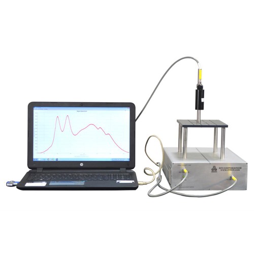
Reflectance Probe |
• Fiberoptics, 400 um fiber core- • with spectrometer leg and Illumination leg
|
Face-Up Measurement |
The film sample faces up with probe and light source pointing down

|
Communication
Interface and
Laptop Computer
|
• USB connector to communicate with PC- • One brand new Laptop with software installed is included for immediate use
|
Software:
TFCompanion
|
• Large library of refractive index (n) and extinction coefficient (k) values for the most
common metallic, dielectric, amorphous and crystalline substrate materials- • Capability for analyzing simple and the most complex film stacks
- • Error estimation and simulation tools allow for factoring in the effects of changing
conditions - • Support for parameterized materials with approximations representing optical
dispersion in a desired spectral range using few coefficients that can be adjusted
-
 
|
| Software Option | - • Remote control (TCP) based on Modbus protocol at extra cost
|
Measurement Standard
(Included) |
• Bare Si Reference and 200 nm thickness silicon oxide test wafer are included as thin
film standards for thickness measurement verification
-
 
|
Dimensions | - • 205 mm L x 250 mm W x 105 mm H (8" L x10" W x4" H)
|
Net Weight | |
Shipping Dimensions | - • 460 mm L x 460 mm W x 460 mm H (18" L x18" W x 18" H)
|
Shipping Weight | |
Warranty
|
- • One year limited warranty with lifetime support. (Consumable parts such as thin film
measurement standard not covered by the warranty)
|
Operation Instruction |
 
|
Application Note
|
An example of metal thin film thickness measurement using the reflectance spectrometer can be downloaded here (Click Pic below)

|