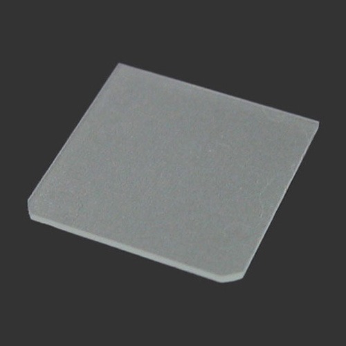
Single crystal quartz wafer is an excellent substrate for microwave filters for wireless communication industries.
MTI can provide high quality quartz wafers for both research and industries production at the lowest price.
Typical Physical Properties
PurityWt %
•SAW grade: > 99.9 •Optical grade: 99.99
Crystal Structure
Hex.a = 4.914 Åc = 5.405 Å
Growth Method
Hydrothermal
Hardness
7.0 Moh’s
Density
2.684 g/cm3
Melt Point
1610 oC( phase transition point: 573.1 oC )
Specific heat
0.18 cal/gm
Thermoelectric Constant
1200 mV /oC @ 300 oC
Thermal conductivity
0.0033 cal/cm/ oC
Thermal expansion (x10-6/ oC)
•a11: 13.71 •a33: 7.48
Index of Refraction
1.544
Q value Acoustic velocity, SAW Frequency constant, BAW Piezoelectric coupling ,
•1.8 x 10⁶ min. •3160 ( m/sec ) •1661 ( kHz/mm ) •K2 (%) BAW: 0.65SAW: 0.14
Inclusion
IEC Grade II
Standard Quartz Wafer Specifications
Orientation
•Y, X or Z cut: Rotated to any value in the range 30o ~ 42.75o ± 5 min. •Primary flat: orientation specified by customer ± 30 min •Secondary Flat: orientation specified by customer. •Seed: located in the center: width < 5mm, height > 66mm
Polished surface
•EPI polished on one side or two sides to Ra < 10 Å •Working Area: Wafer diameter minus 3 mm •BOW: < 20 mm for 3” wafer and 30 mm for 4” wafer •No chips out on working area. In the edge, chip width < 0.5 mm •Pit and scratches: < 3 per wafer or < 20 per 100 wafers
Standard Thickness
•0.5 mm ± 0.05mm •TTV < 5 mm
Standard Diameter
•f 2” (50.8mm )f 3” (76.2mm)f 4” (100mm) ±0.2 mm •Primary Flat : 22 ± 1.5 mm (f 3” ) 32 ± 3.0 mm ( f 4” ) •Secondary Flat: 10 mm ±1.5 mm
Production Capability
20,000 wafer per month
Special size and orientation are available upon request