| |
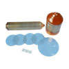
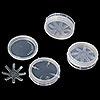
Thermal Oxide Wafer 2" Dia.
Thermal Oxide Wafer: 300 nm SiO2 Layer on Si (100), 2" dia x 0.50 mm t, P type B doped, 1 side polished,R:0.001-0.005 ohm.cm
Thermal oxide Layer Silicon Wafer Specifications - • Conductive type: P type/ Boron doped
- • Resistivity: 0.001- 0.005 ohm-cm
- • Size: 50.8 diameter +/- 0.5 mm x 0.50 +/- 0.025 mm
- • Orientation: (100) +/- 1o
- • Polish: one side polished
- • Surface roughness, Ra: < 5A (RMS)
|