SOS (silicon on Sapphire)

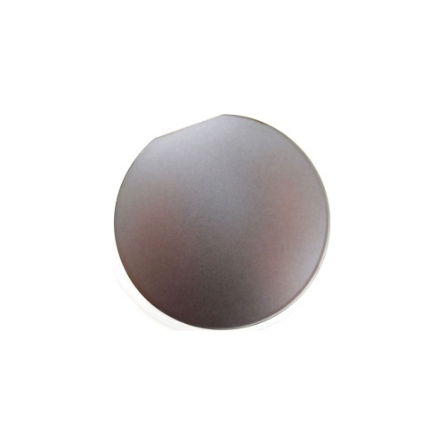
Silicon-on-Sapphire (11-02, R Plane ), 100mm Dia x 0.46mm,2sp, Film: 0.6 um thick

Silicon-on-Sapphire (11-02, R Plane ), 100mm Dia x 0.46mm,2sp, Film: 0.6 um thick

기본 정보
Product Name Silicon-on-Sapphire (11-02, R Plane ), 100mm Dia x 0.46mm,2sp, Film: 0.6 um thick
Sale Price Call for Price
Product Code FmSOS100DD046C2FT06US
Quantity 수량증가수량감소
상품 옵션
 

     Silicon on sapphire (SOS) is a
hetero-epitaxialprocess for integrated
     circuit
manufacturing  that consists of a thin layer (typically thinner than
     0.6 micrometres) of silicongrown on a sapphire (Al2O3) wafer. SOS is
     part of the Silicon on Insulator (SOI) family of CMOS  technologies.
     SOS is primarily used in aerospace and militaryapplications because of its
     inherent
 
resistance to radiation.
 
     U.S. Dept. of Commerce requires End User Certificate for exporting this product.
     Oversea end users must file the end user certificate form (click to download) and
     all sales are subject to get approval by U.S. Dept. of Commerce before shipping.


     SOS(Silicon on Sapphire) Wafers  
    (DSP-Double sides polished)  

     Silicon EPI Layer

  •      •  Silicon Orientation: (100)
  •      •  Type, Dopant:  Intrinsic type, undoped
  •      •  Silicon Thickness: 0.6 um +/- 10%
  •      •  Resistivity: > 100 ohm.cm
  •      •  Micro-particle density ( for particles > 2 um) < 2/cm^2

     Sapphire Wafer
       
  •      •  R plane -- (1-102)  with  single flat
          Purity:  99.996%
  •      •  Wafer size:   100 mm  dia x 0.46 mm thickness 
  •      •  Flat : One flat 32.5mm +/-2.5mm, at 45+/- 1 deg CCW from <C> on <R>
  •      •  Front surface: Epi-polished (Ra < = 0.3 nm)
  •      •  Back surface: Optical grade polish
  •      •  TTV < 15 um, Bow < 20 um, Warp < 20 um, Flatness (TIR) < 12 um,
             with Laser Mark on wafer back-side, just below the Flat