|
|||
|
|
|
|


|
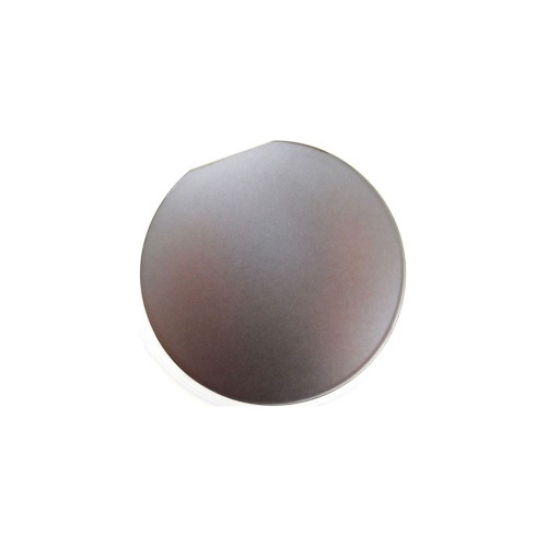
Silicon on sapphire (SOS) is a hetero-epitaxialprocess for integrated circuitmanufacturing that consists of a thin layer (typically thinner than 0.6 micrometres) of silicongrown on a sapphire (Al2O3) wafer. SOS is part of the Silicon on Insulator (SOI) family of CMOS technologies. SOS is primarily used in aerospace and militaryapplications because of its inherent resistance to radiation. U.S. Dept. of Commerce requires End User Certificate for exporting this product. Oversea end users must file the end user certificate form (click to download) and all sales are subject to get approval by U.S. Dept. of Commerce before shipping. SOS(Silicon on Sapphire) Wafers Silicon EPI Layer
Sapphire Wafer
|
||
 Working days : Monday to Saturday 
 |
|||